Photovoltaic (PV) Solar Panels generate electricity by the Photovoltaic Effect. Discovered in 1839 by 19 year old Edmund Becquerel, the photovoltaic effect is the phenomenon that certain materials produceelectic current when they are exposed to light.
PN Junction Semiconductors
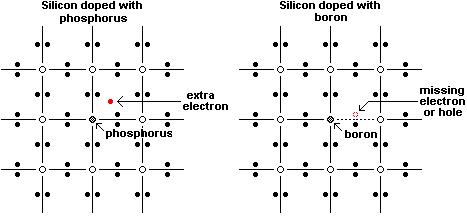
For traditional PV solar panels two halves of one pure silicon crystal are doped with two differentdopants (e.g. arsenic, gallium, aluminium, phosphorus). One half of the crystal is left electron deficient– i.e. the atoms it contains are short of electrons. This is called the p-type layer. The other half of the crystal has an excess of electrons – this is called the n-type layer.
Since one half of the crystal has a lot of electrons, and the other half does not, there is an electric fieldacross the junction between the two halves. Electrons in the crystal can only travel in one direction – from the electron rich half to the electron poor half.
Where the two halves of the crystal meet is called a PN junction, and this doped crystal is a semiconductor. (Click here to read our article How are Solar Panels Made in which the solar panel manufacturing process is presented.)
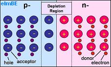
Pictured above is a representation of PN junction semiconductor. The half labelled p- has a shortage of electrons so contains acceptor atoms each with a hole which could be ‘filled’ by an electron. The half labelled n- has excess electrons and so contains donor atoms which have an extra electron.
The Depletion Region
Where the two halves of the crystal meet, there is a depletion region, so called because it is depleted of charge carriers (the electrons and holes). Here electrons have moved from the n-type (negative) side to the p-type (positive) side of the crystal recombining with holes. Likewise holes have moved from the p-type side to the n-type side.
As the silicon atoms themselves do not move, any holes which remain uncovered by electrons in the n-type side are left positively charged, and any electrons without holes to cover in the p-type side remain negatively charged. This leaves positive material close to the junction in the n-type side, and negative material close to the junction in the p-type side with a potential between the two sides of around 0.6-0.7 volts in a silicon PN junction.
With this equilibrium position reached there are two equal and opposite electric currents flowing – holes in one direction and electrons in the other direction – across the depletion region.
Energy from Sunlight
The light from the sun is made up of packets of energy called Photons. Each photon carries an amount of energy corresponding to its wavelength of light.
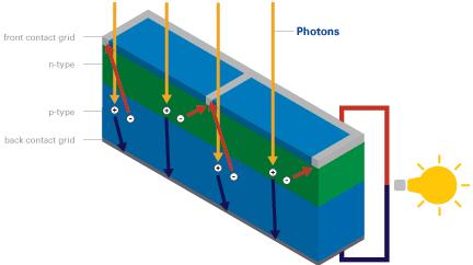
When a visible light photon strikes a solar cell it can do one of three things: pass straight through, be reflected, or be absorbed. If the photon is absorbed, its energy is absorbed by an electron in an atom of the solar cell enabling it to escape from its normal position (photon excitation), cross the junction and fill a hole. Since electrons are physically moving across the PN junction, the positive charge carryingholes are effectively moving in the opposite direction around the load circuit (a rechargeable battery or light bulb etc). This completes the circuit providing more holes for the electrons to combine with and providing usable electricity.
Energy from the sun can be extracted in this way using a standard solar cell at an efficiency of around 5-15% (see our article 40% Efficiency Solar Panels for details on how more efficient solar cells can be made). This process can be repeated over and over again over the many decades of usable lifetime of solar cells.